Posts

Showing posts from May, 2023

PHY622X BLE SoC from PHYPLUS

Image
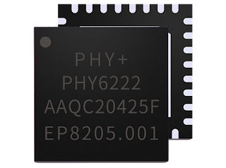
About PHYPLUS PHY622X BLE SoC is manufactured by PHYPLUS Shanghai, a leading advanced BLE SoC supplier in China. Key Features for PHY6222 Cortex-M0 with SWD (only for debug) 128KB-8MB flash memory 64KB SRAM, retention in sleep mode 4-way instruction cache with 8KB cache RAM 96KB ROM (BLE/BLE Mesh stack) 256bit efuse 22 GPIOs GPIO retention in off/sleep mode IO MUX function mapping All pins can be configured for wake-up All pins for triggering interrupt 3x QDEC 6x PWM 2x PDM/I2C/SPI/UART 4x DMA 8x 12bit ADC with low noise voice PGA 6x 24bit timer, one watchdog timer RTC (w/o calendar) Operating range: 1.8 to 3.6V Embdeed buck DC/DC and LDOs battery monitor RC oscillator hardware calibrations Support BLE 2Mbps protocol Support Data Length Extension Throughput up to 1.6Mbps BLE 5.1 Support SIG-Mesh Multi-Feature 2.4GHz transceiver -103dBm @ BLE 125Kbps TX power -20 to _10dBm in 3dB steps AES-128 encryption Link layer hardware Operation temperatrue: -40 to 125 degree RoHS package: QFN32 Re

PY32F0XX Low Cost TSSOP ARM Cortex-M0+ Microcontroller

Image
PY32F030 and PY32F003 are manufactured by PUYA Shanghai, who was known as a low cost SPI flash supplier. High performance 32-bit ARM Cortex-M0+core and MCU with wide voltage operating range are adopted. The maximum embedded memory can reach 64K bytes flash and 8K bytes SRAM, and the maximum operating frequency can reach 48MHz. It contains a variety of different packaging types and products. The chip integrates multiple I2C, SPI, USART and other communication peripherals, one 12bit ADC, six 16bit timers, and two comparators. The operating temperature range is -40 ℃~85 ℃, and the operating voltage range is 1.7V~5.5V. The chip provides sleep and stop low-power operation modes, which can meet different low-power applications. Key features: 32bit ARM Cortex-M0+ core Up to 64KB (embedded) flash memory Up to 4KB SRAMClock subsystem for HSI/HSE/LSI/LSE/PLL Clock up to 48MHz Operating voltage 1.7~5.5V Operating temperature -40~85 Up to 30 GPIOs 1x I2C 2x SPI 2x USART 4x bit GP Timer 1x ADC time

ESP32-C3 WiFi/BLE Multi-mode RISC-V SoC

Image
ESP32-C3 is a multi-mode SoC with WiFi and BLE radios and RISC-V core. This device is manufactured by Expressif in Shanghai. ESP32 is a famous product line for low-cost WiFi/BLE dual mode IoT SoC. The early models are designed with Xtensa LX soft-core. Now Expressif released a RISC-V based version. Its key features: Single core RISC-V SoC running up to 160MHz with 4 level pipelines Built-in 400KB SRAM (16KB cache) 384KB ROM  SPI/Dual SPI/Quad SPI/QPI interfaces to external memories Broad temperature range RSA3072 based security boot, and AES128/XTS256 code protection Digital signature and HMAC modules TRNG True random number generator IEEE802.11 b/g/n 2.4GHz, 20MHz/40MHz bandwidth 1T1R, up to 150Mbps BLE 5 / BLE mesh on 125K/500K/1M/2Mbps 21dBm TX 22 GPIO 3x SPI 2x UART 1x I2C 1x I2S IR transmitter, 2 TX/2RX 6 channel LED PWM Full speed USB serial/JTAG GDMA 1x TWAI for CAN2.06 channel 1x temperature sensor 2x 54bit GP timers 3x watchdog timers 1x analog watchdog timer 1x 52bit systemti

RISC-V MCU GD32VF103 from Giga Devices

Image
GD32VF103 is a RISC-V microcontroller, which is pin to pin compatible to STM32F103. The chip is manufactured by Gigadevices in Shanghai. The key features: 108MHz CPU clock 16 to 128KB flash ROM 6 to 32KB SRAM 1x 16bit advanced timer 4x 16bit general purpose timers 2x 16bit basic timers 1x 24bit systick timer 2x watchdog timer 1x RTC timer 2x UART 3x USART 2x I2C 3x SPI 2x I2S audio interfaces 1x USB OTG 2x CAN 2.0B External memory interface for NOR/SRAM/PSRAM/ROM 2x12bit 16 channel ADC 2x12bit DAC High precision 1Msps ADC 2.6-3.6V, 5V tolerance GPIO, up to 80 I/Os Sleep, deep sleep, standby modes QFN36, LQFP48, LQFP64, LQFP100 Restrictions Mature RISC-V MCU FT2232 based JTAG interface has some restrictions on installation Segger JLINK V10 is working smoothly.

XY1100 CAT-NB SoC from Xinyi (New Wing)

Image
XY1100 is a hybrid NB-IoT SoC with CMOS PA and software radio technologies, developed by Xinyi (New Wing) Shanghai. The key features are: Dual core architecture: MCU + DSP A Cortex-M3 running on 240MHz 900KB RAM and 417KB user flash RX: -134dBm, Tx: 23dBm 690-960MHz, 1.71-2.2GHz QFN52 Support OpenCPU software architecture Support AT modem interface Assessment It is a low cost NB-IoT SoC with software radio and CMOS PA. It can support multiple modem technologies only if you get support from the R&D team. It support on board design, instead of module based design. It has been verified by major operators in China, so its quality is accepted. Recommended for large volume applications. Although it has complete toolchain, but it is key account oriented product, not very friendly to OSHW community.

W801 RISC-V WiFi/BLE combo from Winner Micro

Image
W801 is a WiFi/BLE IoT SoC manufactured by Winner Micro, which is based in Beijing, China. It has rich on-chip peripherals. The key features are: 2.4GHz IEEE802.11b/g/n  Bluetooth/BLE 4.2 dual mode Integrated 32bit C-Sky V2 core General Purpose IO: GPIO/ADC Rich communication interfaces: UART/SPI/I2C Special interface: I2S/7816/SDIO UI interface: LCD/Touch sensor Memory interface: PSRAM Security module: TEE with hardware encryption algorithms Built-in DSP Built-in FPU Code protection 2MB XIP flash memory with code encryption, signature, secure debug, secure OTA GCC support PS: C-Sky V1 was M-core from Motorola semiconductors, and C-Sky V2 was upgraded and revised. Assessment: XIP flash may have some restriction on execution speed and power consumptions. Some time critial code has to run in the RAM ADC precision is low and sampling rate is low. Lack of documentations and supports, although it is quite cheap. A complete SDK/toolchain is ready for OSHW community, but it is helpful for sma

HC32L110 Cortex-M0+ MCU, Low Pin Count, Low Power Consumption, with 12bit 1Msps SARADC

Image
HC32L110 is manufactured by HDSC (Huada Semiconductors). The key features are:  32MHz Cortex-M0+ 32bit MCU Low power consumption 0.5uA @ 3V deep sleep mode 1.0uA @ 3V deep sleep + RTC mode 6uA @32.768kHz slow working mode 20uA/MHz @ 3V @ 16MHz sleep mode 120uA/MHz @ 3V @ 16MHz work mode 3uS ultra low power wakeup mode 16KB/32KB (embedded) flash memory, with write protection 2KB/4KB RAM with verification GPIO 16IO @ 20pin, 12IO @ 16pin Clock and Xtal External high crystal: 4M - 32MHz External low crystal: 32.768KHz Internal high clock: 4/8/16/22.12/24MHz Internal low clock: 32.768K/38.4KHz hardware clock calibration and supervisory circuit. Timer/Counter 3 x 16bit timers/counters 1 x low power 16bit timer/counter 3 x high performance 16bit timers/counters, with PWM complementation and dead-zone protection 1 x programmable 16bit timer/counter, with capture compare and PWM output 1 x 20bit programmable counter/WDT, with independent ultra low power RC-OSC. Communications UART0/UART1 standa